Simulations
2017-2019 Scanning Electron Microscope
Keywords: Semiconductor device simulation, vacuum device simulation, electron beam, SEM image, charging effect, secondary electron emission, FEM, FenicsSummary: Electron beam scans the specimen from the left to the right, from the top to the bottom. Secondary electrons emission are collected and used to generate SEM image. The image is affected by negative or positive charges. For more detail, please read my publications in 2018 [PDF] and 2019 [PDF].
2D simulations:
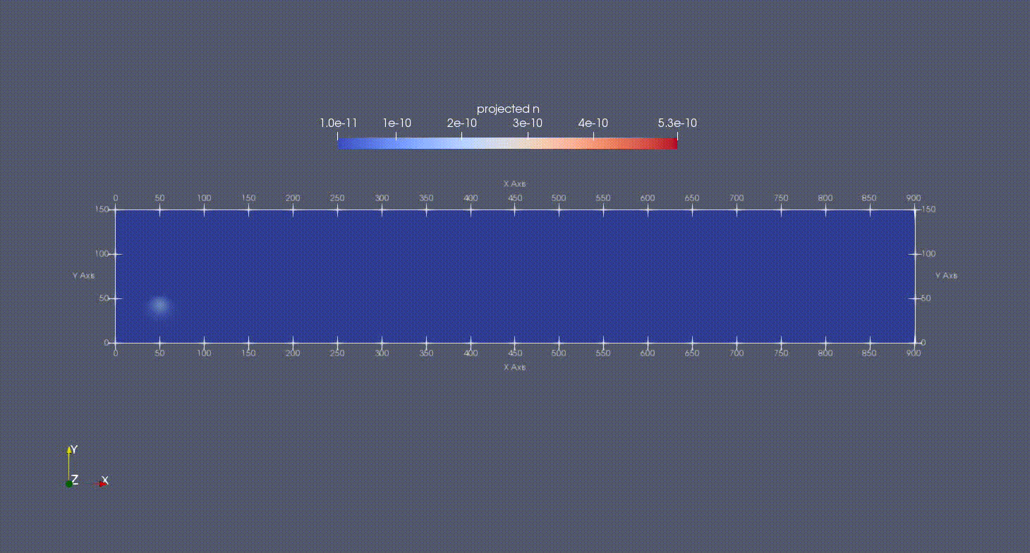
Electron beam scans Si sample
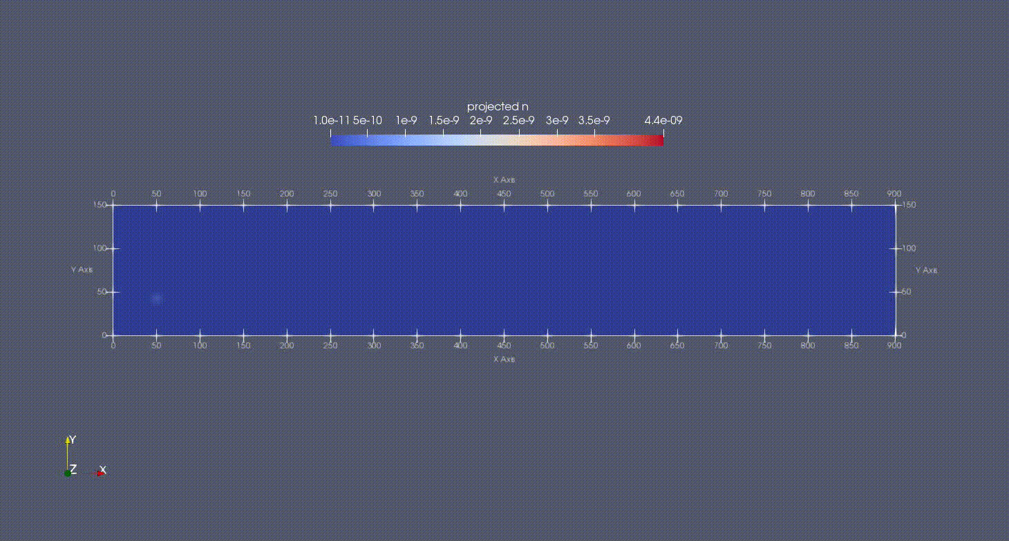
Electron beam scans SiO2 sample
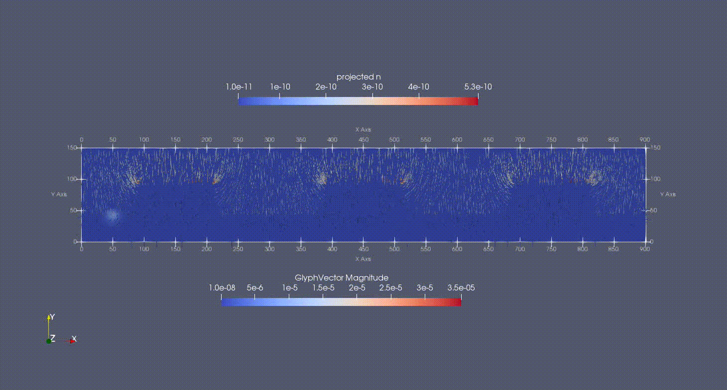
Electrical field during the scanning. Secondary electrons drift toward the electrical field
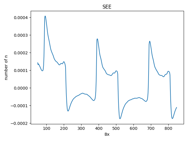
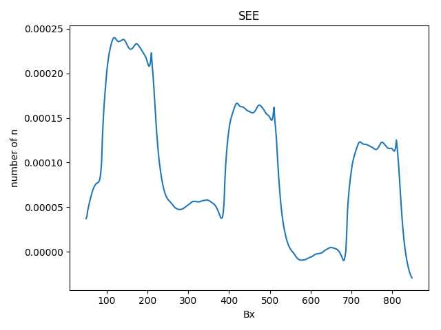
SEE signals from scanning Si and SiO2 samples
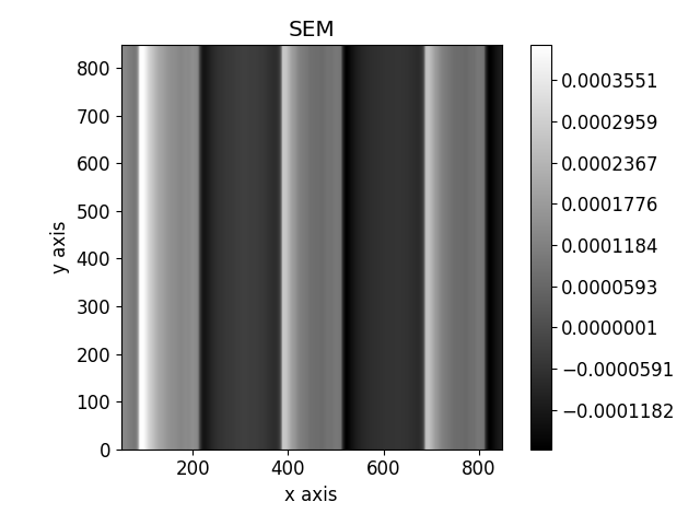
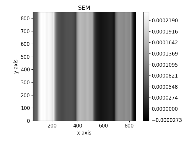
SEM images generated SEE signals
Electron beam scans Si sample
Electron beam scans SiO2 sample
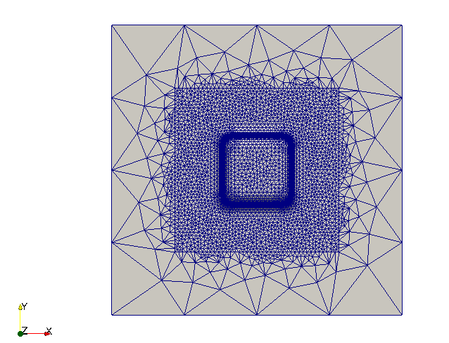
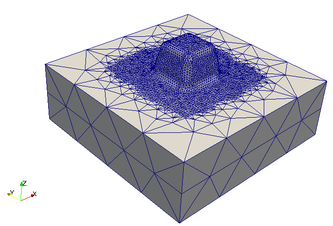
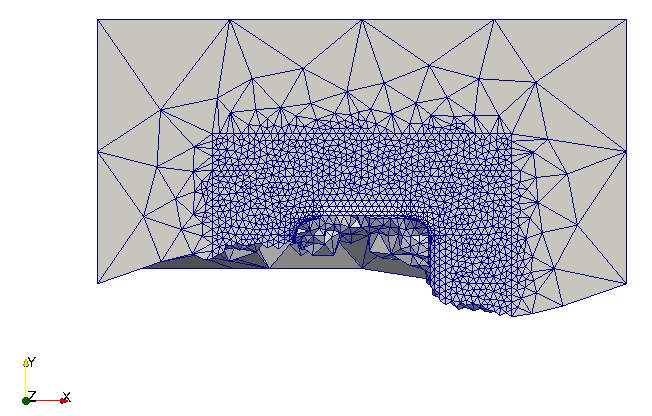
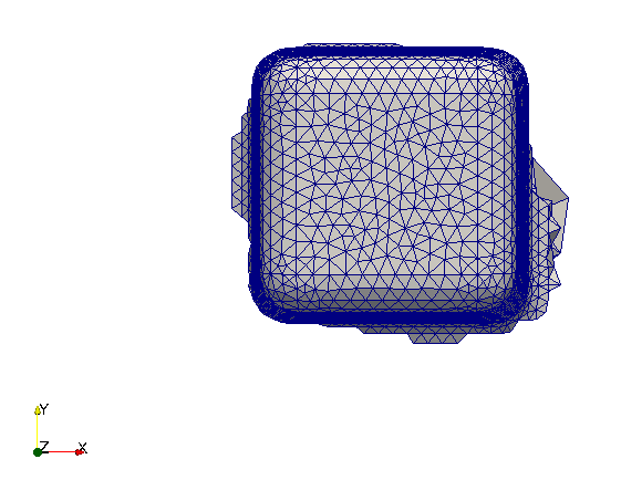
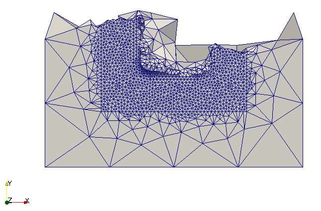
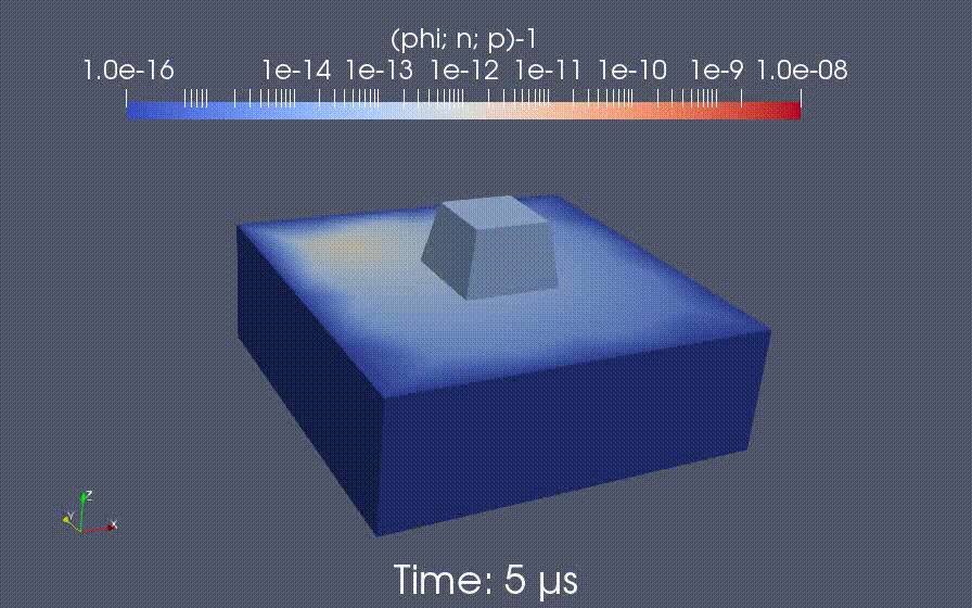
Geometry of a specimen with a pattern in total and in partition for parallel computing
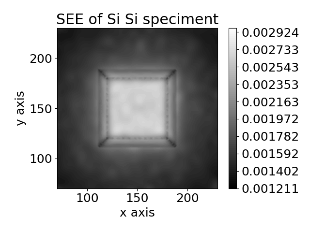
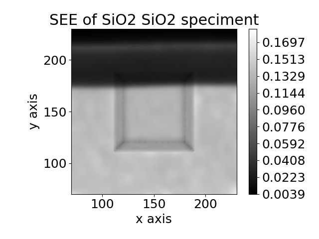
SEM images generated SEE signals